Metal machining for electronics and semiconductor equipment is a specialized manufacturing
field where dimensional accuracy, burr control, surface integrity, cleanliness, and material stability are as
important as machining speed or unit cost. Components often operate in controlled environments such as cleanrooms,
vacuum systems, plasma process chambers, optical inspection platforms, wafer handling modules, and high-density
electronic assemblies.
Searchers looking for this topic usually need practical engineering guidance: which metals are suitable, what
tolerances are realistic, how to specify surface finish, how to reduce particles, how to machine heat-sensitive
or vacuum-critical parts, and how to evaluate a CNC machining supplier for semiconductor or electronics work.
This article addresses those requirements from design, manufacturing, quality, and procurement perspectives.
What Metal Machining Means in Electronics and Semiconductor Equipment
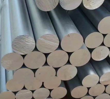
In this market, metal machining usually refers to the subtractive manufacturing of precision parts from aluminum,
stainless steel, copper, titanium, nickel alloys, Kovar, molybdenum, tungsten, and other engineered metals.
Processes include CNC milling, CNC turning, Swiss machining, wire EDM, sinker EDM, grinding, honing, lapping,
deburring, passivation, anodizing, electropolishing, plating, laser marking, and precision cleaning.
Unlike general industrial machining, electronic and semiconductor applications often require tight control over
the entire manufacturing chain. A part may need to be dimensionally stable after anodizing, non-particle-shedding
after repeated handling, compatible with vacuum, resistant to plasma chemistry, thermally conductive, or electrically
grounded through a masked contact surface.
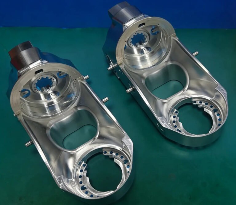
Common machined components
- Vacuum chambers, lids, flanges, gas manifolds, and valve blocks
- Wafer handling arms, end effectors, chucks, pedestals, and support rings
- Heat sinks, cold plates, liquid cooling plates, RF shields, and power electronics housings
- Precision frames, brackets, optical mounts, metrology bases, and alignment stages
- Connector housings, sensor bodies, test sockets, pogo pin fixtures, and probe station parts
- Cleanroom-compatible jigs, fixtures, trays, carriers, and assembly tooling
- Electrostatic chuck components, ceramic-to-metal interface parts, and RF delivery hardware
Why Semiconductor Machining Is More Demanding Than General CNC Work
Semiconductor equipment manufacturing places strict requirements on contamination control, repeatability, and
traceability. A small burr, embedded abrasive, or uncontrolled coating thickness can cause yield loss, wafer defects,
vacuum leaks, misalignment, or premature tool maintenance.
The best suppliers for semiconductor equipment machining understand that a drawing tolerance is
only one part of the requirement. They also manage tool wear, coolant residue, oxide formation, sharp-edge break,
part marking, packaging material, and cleaning method. For vacuum or cleanroom parts, process discipline may matter
as much as machine capability.
| Requirement Area | Typical Semiconductor Concern | Machining Implication |
|---|---|---|
| Particles | Wafer contamination, yield loss, tool downtime | Burr-free edges, controlled deburring, ultrasonic cleaning, clean packaging |
| Vacuum performance | Outgassing, virtual leaks, unstable process pressure | Proper venting, smooth internal surfaces, compatible materials and finishes |
| Thermal stability | Dimensional drift, alignment error, uneven heat transfer | Stress relief, flatness control, matched CTE materials, precise mating surfaces |
| Electrical function | Grounding, shielding, RF loss, insulation failure | Masked coating areas, conductive finishes, tight contact geometry |
| Chemical resistance | Corrosion from process gases or cleaning chemicals | Material selection, passivation, electropolishing, suitable coating stack |
Material Selection for Electronics and Semiconductor Machined Parts
Material choice directly affects machinability, cost, cleanliness, thermal behavior, and service life.
Electronics and semiconductor equipment frequently require materials with a specific combination of conductivity,
corrosion resistance, magnetic behavior, weight, stiffness, coefficient of thermal expansion, and compatibility with
finishing processes.
| Material | Why It Is Used | Machining and Design Notes |
|---|---|---|
| Aluminum 6061-T6 | Good machinability, low weight, moderate cost, anodizing compatibility | Common for frames, housings, brackets, cold plates, and tooling; coating thickness must be considered |
| Aluminum 7075-T6 | Higher strength than 6061, good stiffness-to-weight ratio | Used for structural parts; corrosion protection and stress relief may be important |
| Stainless Steel 304/316L | Corrosion resistance, vacuum compatibility, strength, cleanability | Used for chambers, fittings, shafts, and chemical-exposed parts; 316L is preferred for harsher environments |
| Copper C101/C110 | High thermal and electrical conductivity | Used for heat spreaders, RF parts, electrodes, bus bars; prone to burrs and deformation if poorly fixtured |
| OFHC Copper | High-purity copper with low oxygen content | Often used in high-vacuum, RF, and thermal applications; surface handling is critical |
| Titanium Grade 2/5 | High strength-to-weight ratio, corrosion resistance, low thermal conductivity | Used where chemical compatibility or weight reduction is needed; requires careful heat control while cutting |
| Kovar | Controlled thermal expansion close to glass or ceramics | Used in hermetic packages, feedthroughs, and optoelectronics; heat treatment history matters |
| Molybdenum and Tungsten | High-temperature stability, stiffness, low vapor pressure | Used for deposition, ion implantation, and high-temperature fixtures; often requires grinding or EDM |
| Nickel Alloys | Corrosion and heat resistance | Useful in aggressive environments; lower machinability increases cost and lead time |
Engineering note: aluminum vs. stainless steel for semiconductor equipment
Aluminum is preferred when weight, thermal conductivity, and machining cost are key factors. It is commonly
anodized for wear and corrosion resistance. Stainless steel is preferred when chemical resistance, strength,
vacuum robustness, or cleanability is more important. For vacuum chambers and gas delivery hardware, stainless
steel is often selected because it handles welding, passivation, and leak testing well. For large motion stages
and equipment frames, aluminum can reduce mass and improve dynamic response.
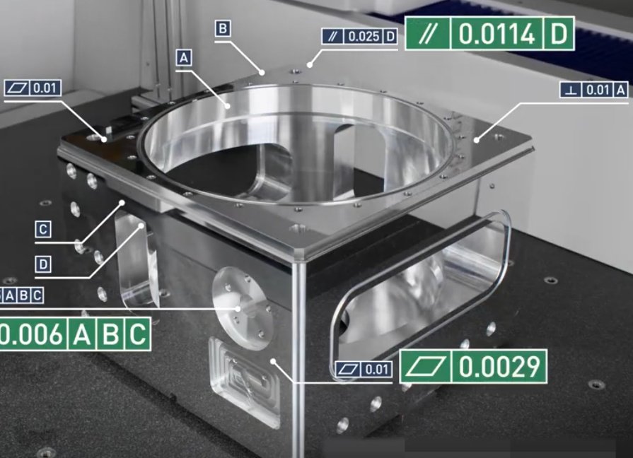
Critical Tolerances, GD&T, and Dimensional Control
Precision machining for semiconductor equipment often involves tolerances tighter than standard commercial CNC
work. However, unnecessarily tight tolerances increase cost, inspection time, scrap risk, and lead time. A good
drawing separates functional dimensions from non-critical features and applies GD&T according to standards such
as ASME Y14.5 or ISO GPS practices.
Common requirements include flatness for sealing or thermal transfer, perpendicularity for alignment, positional
tolerance for dowel holes, concentricity or runout for rotating components, and surface profile for precision
interface planes. Large aluminum plates may also require stress-relieved material and controlled machining sequences
to prevent warping.
| Feature Type | Typical Requirement Range | Engineering Consideration |
|---|---|---|
| Dowel pin holes | ±0.005 mm to ±0.013 mm depending on fit | Reaming, boring, or jig grinding may be needed for repeatable assembly alignment |
| Sealing surfaces | Flatness from 0.01 mm to 0.05 mm over controlled areas | Machining stress, lapping, and plating thickness can affect final flatness |
| O-ring grooves | Tight width, depth, and surface finish control | Corner radius, gland fill, and compression must match the seal design |
| Optical or metrology mounts | Position and angular control often more important than size alone | Datum structure and inspection setup should match actual assembly conditions |
| Heat transfer interfaces | Flatness and roughness often specified together | Too rough reduces contact area; too polished may not always improve interface performance |
Surface Finish, Coatings, and Cleanliness Requirements
Surface condition strongly affects particle generation, sealing performance, corrosion resistance, electrical
contact, optical stray reflection, and outgassing. Drawings should define surface roughness, edge break, coating
type, masking areas, and final cleaning requirements instead of relying on generic notes.
Typical surface finish references include Ra values such as 3.2 µm, 1.6 µm, 0.8 µm, or finer for sealing and
precision mating surfaces. For vacuum components, internal blind holes, sharp corners, porous coatings, and trapped
residues can contribute to contamination or virtual leak behavior.
Common finishing processes
- Type II anodizing: general corrosion protection and appearance for aluminum components.
- Hardcoat anodizing: improved wear resistance for sliding, handling, and fixture surfaces.
- Electroless nickel plating: uniform deposit, hardness, corrosion resistance, and solderability options.
- Passivation: removal of free iron from stainless steel surfaces to improve corrosion resistance.
- Electropolishing: smoothing and brightening stainless surfaces, often used for cleanliness and corrosion resistance.
- Chem-film conversion coating: corrosion protection for aluminum while maintaining electrical conductivity in selected cases.
- Black oxide or black anodizing: optical reflection control, with compatibility confirmed for the operating environment.
- Nickel, silver, or gold plating: electrical conductivity, RF performance, solderability, or corrosion resistance.
Burr control is a functional requirement, not a cosmetic preference. In semiconductor and electronics
assemblies, burrs can detach as particles, damage cables or seals, create electrical shorts, interfere with motion,
or prevent accurate seating of components. Critical edges should be identified with exact edge-break instructions,
such as “break sharp edges 0.1–0.2 mm unless otherwise specified,” while sealing edges may require no rounding.
Practical specification checklist for surface finish and cleanliness
- Define Ra or Rz where surface function matters.
- Specify coating type, class, color, thickness range, and applicable standard where relevant.
- Identify masked areas for grounding, sealing, bonding, or precision fits.
- Call out “no loose burrs” or controlled edge break on particle-sensitive parts.
- State whether ultrasonic cleaning, solvent cleaning, DI water rinse, vacuum baking, or cleanroom bagging is required.
- Use compatible packaging that does not shed fibers, transfer plasticizer, or corrode the part.
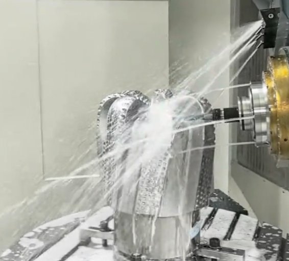
Machining Processes Used for Semiconductor and Electronics Parts
Different machined components require different process routes. A simple aluminum bracket may be finished in one
or two milling operations, while a vacuum chamber may require rough machining, stress relief, finish machining,
welding, leak testing, cleaning, and surface treatment. Process planning affects precision, cost, and risk.
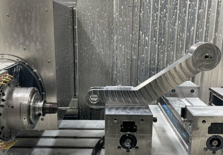
CNC milling
CNC milling is used for plates, frames, housings, heat sinks, cold plates, optical mounts, manifolds, and complex
3-axis or 5-axis parts. Five-axis machining reduces setups, improves datum consistency, and enables complex
semiconductor tooling geometry, but it also requires advanced programming and inspection capability.
CNC turning and mill-turn machining
CNC turning is used for shafts, spacers, sleeves, nozzles, feedthrough bodies, RF connectors, and cylindrical
precision parts. Mill-turn machines can produce cross-holes, flats, threads, grooves, and turned diameters in one
setup, improving concentricity and reducing handling.
EDM and wire cutting
Wire EDM is useful for hard metals, fine profiles, small internal radii, and thin-wall features. It is common in
precision tooling, test fixtures, micro features, and high-temperature materials. EDM recast layer and surface
integrity should be controlled for critical applications.
Grinding, lapping, and honing
Grinding and lapping are used when flatness, parallelism, or surface finish exceed standard milling capability.
These processes are common for precision plates, spacers, ceramic-metal interfaces, sealing surfaces, and metrology
components. Honing is used for accurate bores with controlled geometry and finish.
Thermal Management Components: Heat Sinks, Cold Plates, and Copper Parts
Electronics and semiconductor systems generate significant heat in power modules, RF generators, laser drivers,
motor controllers, power supplies, and process equipment. Machined thermal components must balance heat transfer,
pressure drop, corrosion resistance, leak integrity, flatness, and assembly constraints.
Aluminum heat sinks are commonly CNC machined for prototypes, low-volume production, high-power custom electronics,
and equipment where extrusion cannot provide the required geometry. Copper is selected where thermal conductivity
is the highest priority, but it is heavier, more expensive, and more challenging to machine without burrs or
deformation.
Example engineering result
In one typical power electronics housing redesign, changing from a flat aluminum mounting plate to a CNC-machined
cold plate with internal serpentine channels reduced measured device case temperature by approximately 12–18°C at
the same coolant flow range. The final improvement depended on coolant temperature, channel geometry, interface
material thickness, and clamping pressure. This type of result illustrates why machined thermal parts should be
designed using both mechanical tolerance analysis and thermal simulation.
| Thermal Part | Key Machining Requirement | Typical Risk |
|---|---|---|
| Heat sink | Thin fins, base flatness, surface area, mounting hole accuracy | Fin vibration, tool marks, burrs, insufficient contact area |
| Cold plate | Channel geometry, sealing groove accuracy, flat mating surface | Leakage, trapped chips, excessive pressure drop, warping after brazing |
| Copper spreader | Flatness, low burr, controlled oxidation, proper packaging | Handling dents, surface contamination, unstable contact resistance |
| RF heat sink | Thermal and electrical contact, coating masks, grounding surfaces | Coating on contact pads, poor RF continuity, uneven mounting pressure |
Vacuum, UHV, and Cleanroom-Compatible Machined Parts
Vacuum and ultra-high vacuum components require special design and machining discipline. Common parts include
chambers, lids, flanges, shutters, shields, gas blocks, motion feedthrough components, sample holders, and deposition
system hardware. In these applications, geometry and cleanliness can directly affect pump-down time, base pressure,
process stability, and maintenance frequency.
Design teams should avoid trapped volumes, unvented blind threaded holes, rough internal cavities, and materials
or finishes with high outgassing risk. Welded vacuum assemblies require careful joint design, distortion control,
and helium leak testing. Depending on the application, leak rate requirements may be specified in mbar·L/s or
atm·cc/s, and acceptance criteria should be defined before fabrication.
Vacuum machining considerations
- Use vented screws or vent paths where trapped gas is possible.
- Minimize blind holes, crevices, and rough internal pockets.
- Control weld distortion before final machining of precision interfaces.
- Specify compatible lubricants, coolants, and cleaning processes.
- Use stainless steel, aluminum, titanium, OFHC copper, or refractory metals based on operating conditions.
- Confirm compatibility of anodizing, plating, adhesives, and markings with vacuum level and process chemistry.
Example: preventing a virtual leak in a machined vacuum fixture
A vacuum fixture with multiple blind tapped holes may pass a dimensional inspection but pump down slowly because
gas is trapped behind screw threads. Adding vented holes, through-holes, or flats on screws can create a gas path
and reduce pump-down instability. This is a design-for-vacuum issue rather than a basic machining defect, so it
should be addressed in the drawing and design review stage.
Quality Control and Inspection for Precision Machined Parts
Semiconductor and electronics customers usually require more than a basic certificate of conformance. Inspection
may include first article inspection, CMM reports, material certificates, plating certificates, surface roughness
measurements, hardness testing, helium leak testing, visual inspection under magnification, and cleanliness
documentation.
Inspection planning should follow the actual function of the part. For example, a large frame may
require CMM verification of datum-related hole positions, while a sealing plate may require flatness mapping and
surface roughness checks. A copper bus bar may require conductivity-related material certification and controlled
plating thickness.
| Inspection Method | Used For | Typical Output |
|---|---|---|
| CMM measurement | GD&T, hole patterns, datum relationships, profiles | Dimensional inspection report with measured deviations |
| Optical comparator or vision system | Small profiles, slots, edge conditions, micro features | 2D geometry verification and visual evidence |
| Surface roughness tester | Sealing surfaces, sliding faces, thermal interfaces | Ra, Rz, or other roughness parameters |
| Helium leak test | Vacuum chambers, welded assemblies, sealed cold plates | Leak rate result and pass/fail judgment |
| Coating thickness measurement | Anodizing, nickel plating, conductive coatings | Thickness data, often by XRF, eddy current, or cross-section method |
| Cleanliness inspection | Cleanroom and particle-sensitive hardware | Visual, wipe, particle count, or customer-defined cleanliness record |
Design for Manufacturability: Reducing Cost Without Losing Performance
DFM is especially valuable in precision electronics and semiconductor machining because early design decisions
determine manufacturing risk. A small change to corner radius, pocket depth, datum structure, or coating mask can
reduce cost without reducing function.
High-value DFM recommendations
- Use realistic tolerances; reserve tight tolerances for features that affect alignment, sealing, or electrical function.
- Increase internal corner radii where possible to allow stronger tools and faster machining.
- Avoid deep narrow pockets unless they are functionally required.
- Define datum surfaces based on how the part is assembled and inspected.
- Account for anodizing or plating buildup on holes, slots, and mating faces.
- Use standard stock sizes when possible to reduce material waste and lead time.
- Consider stress relief for large aluminum or stainless components before finish machining.
- Split overly complex parts into assemblies if it improves machining access, cleaning, or serviceability.
- Clearly identify critical-to-quality dimensions instead of applying blanket tight tolerances.
For example, changing a deep 3 mm internal corner radius to 6 mm can allow the use of a more rigid end mill, reduce
chatter, improve surface finish, and shorten cycle time. Similarly, allowing a non-functional pocket floor to remain
at Ra 3.2 µm instead of Ra 0.8 µm can avoid unnecessary finishing operations.
Procurement and Supplier Evaluation for Semiconductor CNC Machining
For procurement teams, the lowest quoted unit price is not always the lowest total cost. Semiconductor
equipment parts can create expensive downstream problems if they arrive with burrs, coating errors, poor packaging,
missing documentation, or uncontrolled dimensional variation. Supplier evaluation should include technical capability,
process control, quality documentation, responsiveness, and experience with clean or vacuum-compatible parts.
Supplier capabilities to verify
- Experience with semiconductor equipment, electronics hardware, cleanroom tooling, or vacuum components
- Multi-axis CNC milling, precision turning, EDM, grinding, and finishing partner network
- Material traceability and ability to provide certificates on request
- CMM inspection, surface roughness measurement, coating inspection, and first article reporting
- Documented deburring, cleaning, and packaging procedures
- Ability to manage small prototype batches and repeat production runs
- Understanding of anodizing masks, plating buildup, and post-finish dimensional effects
- Engineering communication for DFM feedback before production
| Buyer Question | Why It Matters |
|---|---|
| Can the supplier hold tolerance after anodizing or plating? | Coating buildup can close holes, change fits, and affect sealing or grounding surfaces. |
| How are burrs removed from cross-holes and internal channels? | Hidden burrs can become particles or block fluid and gas passages. |
| Can they provide inspection reports for critical dimensions? | High-value equipment builds often require documented dimensional evidence. |
| Do they understand vacuum venting and trapped-volume risks? | Vacuum performance problems may not be visible during basic inspection. |
| How are clean parts packaged and labeled? | Improper packaging can undo cleaning work and introduce fibers, oils, or corrosion. |
Common Engineering Problems and Practical Solutions
Real-world machining problems in electronics and semiconductor equipment are often caused by interactions between
geometry, material, finishing, and assembly requirements. Addressing these interactions early reduces rework and
improves equipment reliability.
| Problem | Likely Cause | Practical Solution |
|---|---|---|
| Flat aluminum plate warps after machining | Residual stress, asymmetric material removal, insufficient roughing strategy | Use stress-relieved stock, rough both sides, allow rest time, finish from stable datums |
| Threads shed particles during assembly | Burrs, galling, rough thread finish, unsuitable cleaning | Use thread forming or controlled tapping, deburr thread starts, clean and inspect under magnification |
| Anodized holes are too tight | Coating buildup not included in design or process plan | Oversize before coating or mask precision bores; verify final dimensions after finish |
| Cold plate leaks after assembly | Poor sealing groove geometry, flatness issue, trapped chips, inadequate test plan | Control O-ring groove dimensions, clean internal channels, pressure test or helium leak test |
| Vacuum part has long pump-down time | Virtual leaks, rough internal surfaces, trapped cleaning fluids | Add vent paths, avoid blind cavities, specify vacuum cleaning and drying requirements |
| Electrical grounding fails after coating | Insulating anodize or paint covers contact area | Define masked conductive surfaces and inspect coating boundaries |
Key Standards and Reference Points
Machined parts for electronics and semiconductor equipment may reference several standards depending on industry,
geography, customer requirements, and application. Not every part needs every standard, but using recognized
references improves communication and reduces ambiguity.
- ASME Y14.5: widely used for geometric dimensioning and tolerancing.
- ISO 1101: international standard for geometrical product specifications and GD&T concepts.
- ISO 2768: general tolerances for linear and angular dimensions where specific tolerances are not stated.
- ISO 9001: quality management system standard often required by equipment manufacturers.
- ASTM material specifications: commonly used for defining metal grades and material requirements.
- MIL-A-8625 / MIL-PRF-8625: commonly referenced for anodic coatings on aluminum.
- ASTM A967: chemical passivation treatments for stainless steel parts.
- SEMI standards: relevant in semiconductor manufacturing environments for areas such as safety, facilities, materials, and equipment practices.
Conclusion
Metal machining for electronics and semiconductor equipment requires more than accurate CNC programming. The best
outcomes come from aligning material selection, tolerance strategy, surface finish, coating control, cleanliness,
inspection, and packaging with the actual operating environment of the part.
Engineers should specify functional requirements clearly, including datum structure, critical dimensions, surface
finish, edge condition, coating masks, and cleanliness expectations. Buyers should evaluate machining suppliers by
their ability to control process risk, provide documentation, and understand semiconductor-specific issues such as
particles, vacuum behavior, thermal stability, and post-finish dimensional changes.
When these factors are managed correctly, precision machined metal components improve semiconductor tool uptime,
electronic system reliability, thermal performance, assembly repeatability, and long-term equipment value.